48 V → 12 V GaN Point-of-Load Converter
A 300 W synchronous buck built around 100 V GaN half-bridges, designed for high density and a clean switching node under load transients.

Overview
Intermediate bus converters on a dense avionics stack are usually thermally limited long before they are electrically limited. This board was an attempt to move that limit: 100 V GaN half-bridges, a two-phase interleaved synchronous buck, and a layout organized entirely around minimizing the high-di/dt loop area so that the switching node stays clean enough to run at 500 kHz without a snubber.
| Year | 2025 |
| Role | Design lead — schematic, layout, magnetics, firmware, bring-up |
| Disciplines | Power Electronics, PCB Design, Modeling & Simulation, Embedded Firmware |
Requirements
The converter feeds a 12 V rail shared by motor drivers and a compute module, so it has to hold regulation through a load step that is a large fraction of full load, and it has to do so inside a sealed enclosure with conduction cooling only.
Requirement set
| Input range | 36 – 60 V DC (48 V nominal) |
| Output | 12 V ± 2 % static, ± 5 % transient |
| Load | 0 – 25 A continuous, 40 A for 100 ms |
| Transient | 0 → 20 A at 10 A/µs, < 400 mV deviation |
| Efficiency | > 95 % from 30 % to 100 % load |
| Cooling | Conduction only, 70 °C baseplate |
| Envelope | 70 × 45 × 12 mm including magnetics |
Topology selection
A 4:1 step-down at 25 A is comfortably inside the range where a synchronous buck wins, so the interesting decision was not which topology but how many phases. Single-phase at 500 kHz put the inductor ripple and the output capacitor RMS current above what I wanted in a conduction-cooled enclosure. Two interleaved phases cut input capacitor RMS current by roughly half and moved effective output ripple to 1 MHz, which let the output filter shrink faster than the extra phase cost in area.
I built the same trade study into an interactive tool on this site — see the topology selector and the buck design calculator.
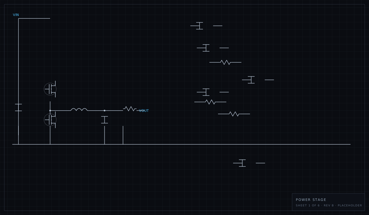
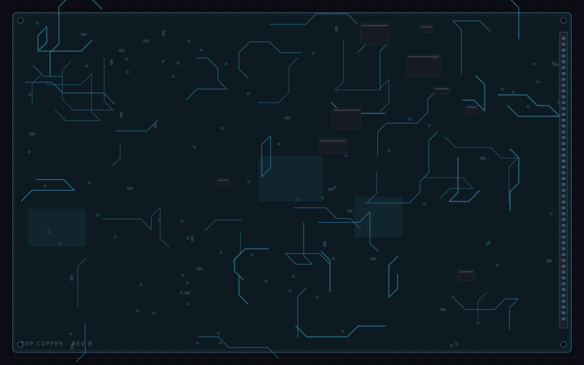
Select a numbered marker for the design rationale behind that region.
Control and firmware
Peak current-mode control with slope compensation, closed digitally on an STM32G4 so the compensator could be retuned in the lab without spinning a board. The ADC sample point is aligned to the middle of the low-side conduction interval to reject switching noise, and a fault state machine latches the gate drives off on overcurrent, overtemperature, or a missing phase.
/* Peak current-mode inner loop. Runs in the ADC EOC ISR, phase-aligned to
 * the middle of the low-side conduction interval so the sample lands away
 * from the switching edge. Fixed point Q15 to keep the ISR under 400 ns. */
void ctrl_isr(void)
{
    const q15_t i_sense = adc_read_q15(ADC_ISENSE);
    const q15_t v_out   = adc_read_q15(ADC_VOUT);

    /* Outer voltage loop runs at 1/16 rate; inner loop uses its last output. */
    if (++s_tick >= 16u) {
        s_tick = 0u;
        s_i_ref = pi_update(&s_v_comp, VOUT_REF_Q15 - v_out);
        s_i_ref = q15_clamp(s_i_ref, 0, I_LIMIT_Q15);
    }

    /* Slope compensation: subtract a ramp proportional to elapsed on-time. */
    const q15_t ramp  = q15_mul(SLOPE_Q15, (q15_t)TIM1->CNT);
    const q15_t error = s_i_ref - (i_sense + ramp);

    q15_t duty = pi_update(&s_i_comp, error);
    duty = q15_clamp(duty, DUTY_MIN_Q15, DUTY_MAX_Q15);

    if (fault_pending()) {
        pwm_force_safe_state();   /* both gates low, latch until cleared */
        return;
    }

    pwm_set_duty_interleaved(duty);
}Measured results
What I would change
The DCR sense network is the weakest part of the design — it is accurate enough for current limit but its tolerance over temperature makes phase-current sharing worse than it needs to be. On a second revision I would spend the area on inline shunts with a dedicated amplifier per phase. I would also move the gate drive supply to a fully isolated rail; bootstrapping worked, but it constrains how long the converter can sit at very high duty cycle during a brownout.
Questions about this design? I am happy to walk through the trade studies, the measurements, or anything I glossed over here — drakeajoseph@gmail.com.